
2026 World Cup spotlights UN warning as 40% of Earth’s land is degraded
As the 2026 FIFA World Cup draws global attention to football pitches, the United Nations ...

Samsung Electronics plans to invest about KRW 20 trillion by 2028 in a new semiconductor research and development facility in Giheung, South Korea, aiming to extend its leadership in state-of-the-art semiconductor technology.
The new facility – to be set up on an area covering about 109,000 square meters within its Giheung campus – will lead advanced research on next-generation devices and processes for memory and system semiconductors, as well as development of innovative new technologies based on a long-term roadmap.
The groundbreaking ceremony was attended by Samsung Electronics Vice Chairman Jay Y. Lee, President and CEO Kye Hyun Kyung, President of the Memory Business Jung-Bae Lee, President of the Foundry Business Siyoung Choi and President of the S.LSI Business Yong-In Park, along with more than 100 employees.
“Our new state-of-the-art R&D complex will become a hub for innovation where the best research talent from around the world can come and grow together,” said President Kye Hyun Kyung, who also heads the Device Solutions (DS) Division. “We expect this new beginning will lay the foundation for sustainable growth of our semiconductor business.”
With the establishment of the new R&D facility, Samsung Electronics is seeking to overcome the limits of semiconductor scaling and solidify its competitive edge in semiconductor technology.
The new Giheung R&D facility, together with the R&D line in Hwaseong and the world’s largest semiconductor production complex in Pyeongtaek, is also expected to elevate the synergy among Samsung’s three main semiconductor complexes in the metropolitan area.
As the 2026 FIFA World Cup draws global attention to football pitches, the United Nations ...
Deutsche Bank is stepping up its sustainable aviation strategy by investing in approximately 1,600 metric ...
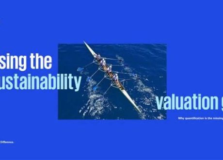
Sustainability has become a core business priority for companies worldwide, with half of organizations now ...

Leave a comment